PCB Layout Design: Step-by-Step Guide for Beginners A guide to the rf pcb design
If you are looking for Story Design: Step by Step you've came to the right place. We have 25 Pics about Story Design: Step by Step like PCB Layout design | FX PCB, [PDF] Intro to PCB Design: A Beginner’s Guide to Mastering PCB Layout and also How to Design a PCB Layout. Here it is:
Story Design: Step By Step
 studentpress.org
Story Design: Step by Step
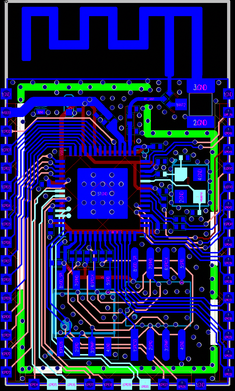
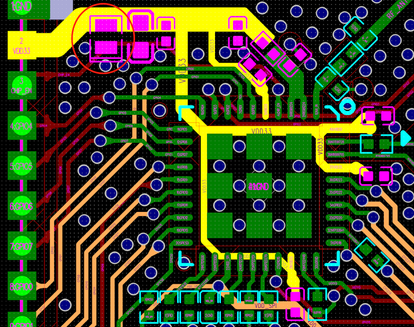
PCB Layout Design - ESP32-C6 - — ESP Hardware Design Guidelines Latest
 docs.espressif.com
PCB Layout Design - ESP32-C6 - — ESP Hardware Design Guidelines latest ...
A Detailed Guide To PCB Layout Design - IBE Electronics
 www.pcbaaa.com
A detailed guide to PCB layout design - IBE Electronics
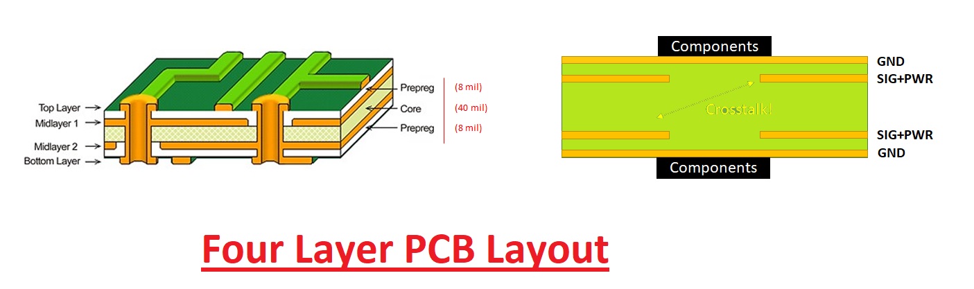
Four Layer PCB Layout: Design Process And Cost Of Manufacturing
 hackaday.io
Four Layer PCB Layout: Design Process and Cost of Manufacturing ...
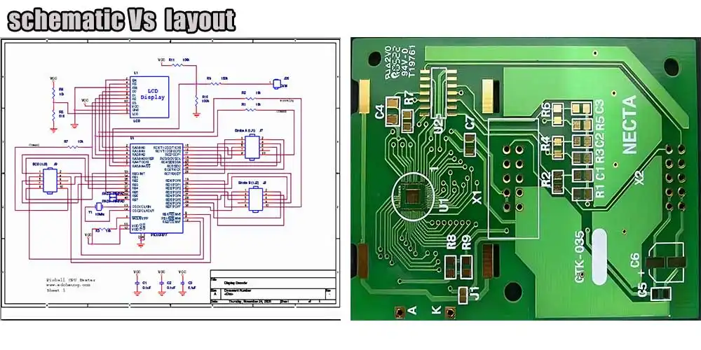
PCB Layout Design | FX PCB
 sfxpcb.com
PCB Layout design | FX PCB
Story Design: Step By Step
 studentpress.org
Story Design: Step by Step
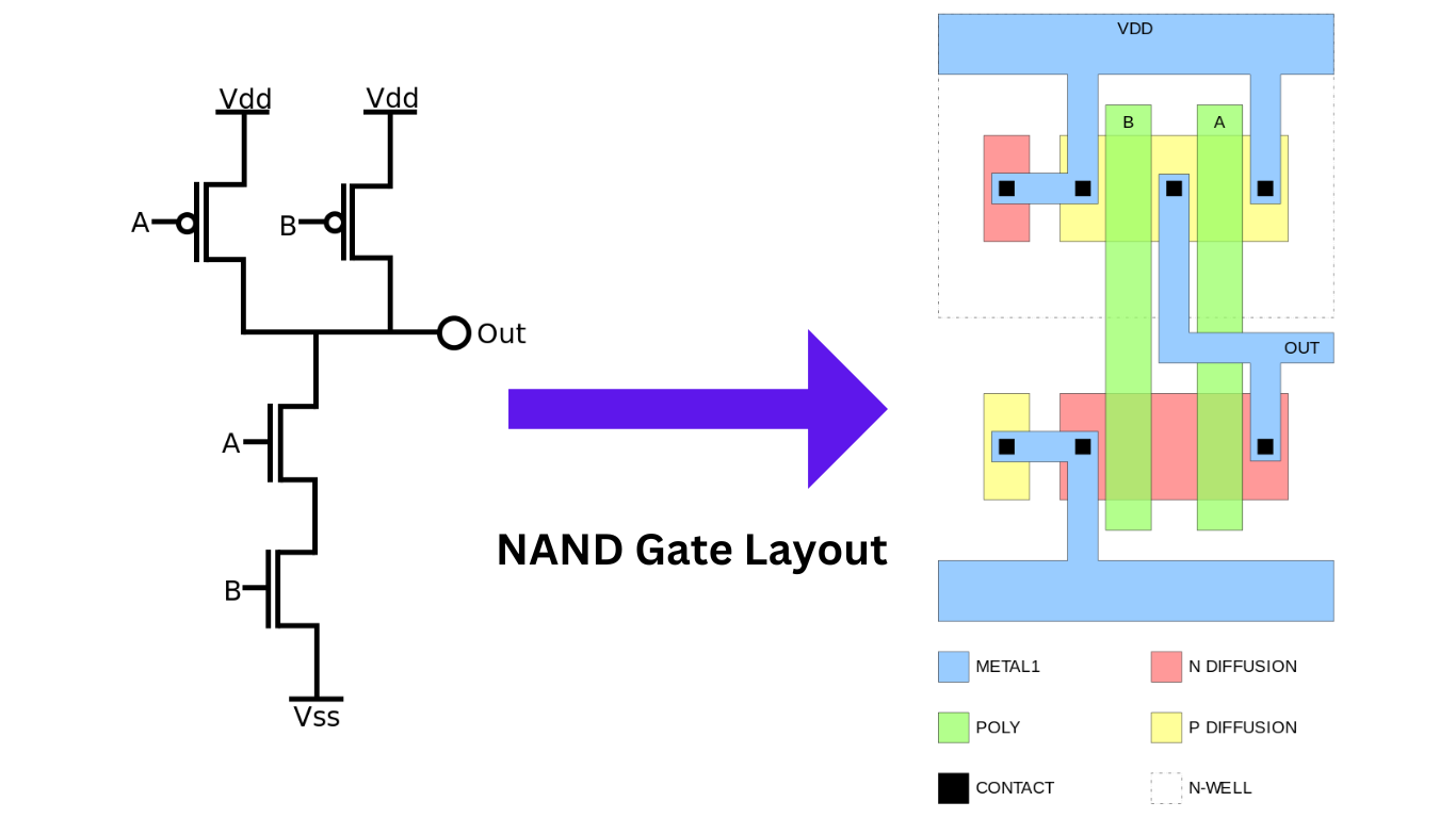
Nand Gate Cmos Diptrace Pcb Layout
 mavink.com
Nand Gate Cmos Diptrace Pcb Layout
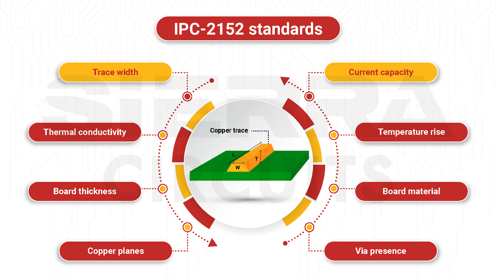
Optimize Your PCB Trace Using IPC-2152 Standard | Sierra Circuits
 www.protoexpress.com
Optimize your PCB trace using IPC-2152 standard | Sierra Circuits
Step-by-step Cadence PCB Design Tutorial - RayPCB
 www.raypcb.com
Step-by-step cadence PCB design tutorial - RayPCB
Mobile App Design: Step-by-step Guide
 www.linkedin.com
Mobile app design: Step-by-step guide
Step-by-step Cadence PCB Design Tutorial - RayPCB
 www.raypcb.com
Step-by-step cadence PCB design tutorial - RayPCB
Complete Guide To PCB Layout Design Steps And Rules – PCB HERO
 www.pcb-hero.com
Complete Guide To PCB Layout Design Steps And Rules – PCB HERO
PCB Design Engineer Resume Sample (2023)
 itchol.com
PCB Design Engineer Resume Sample (2023)
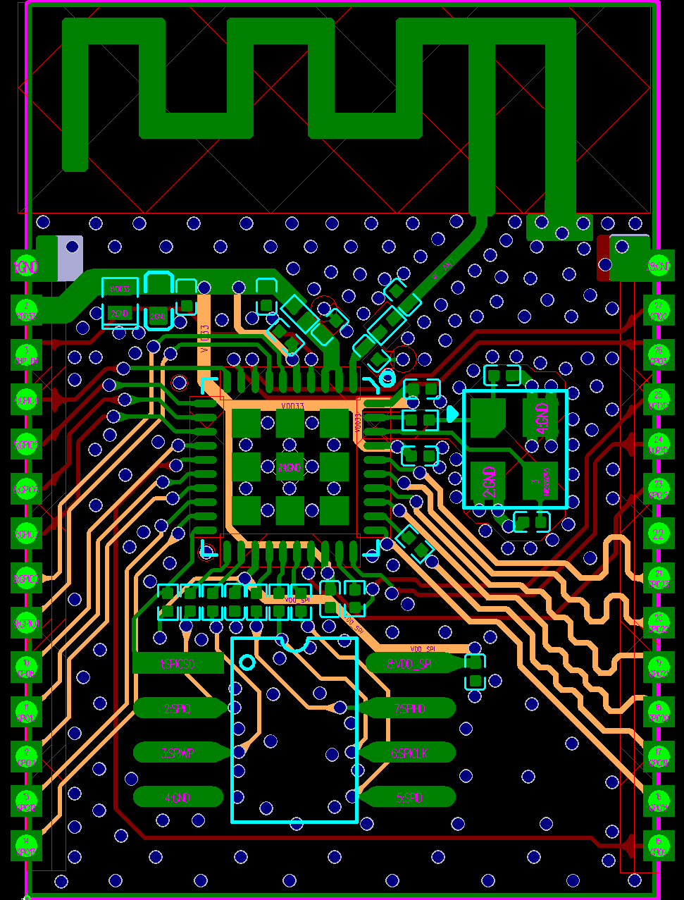
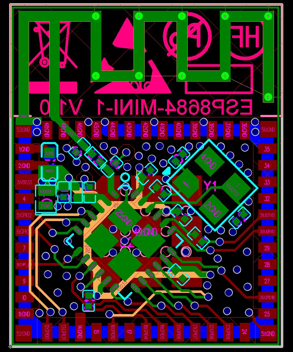
PCB Layout Design - ESP32-S2 - — ESP Hardware Design Guidelines Latest
 docs.espressif.com
PCB Layout Design - ESP32-S2 - — ESP Hardware Design Guidelines latest ...
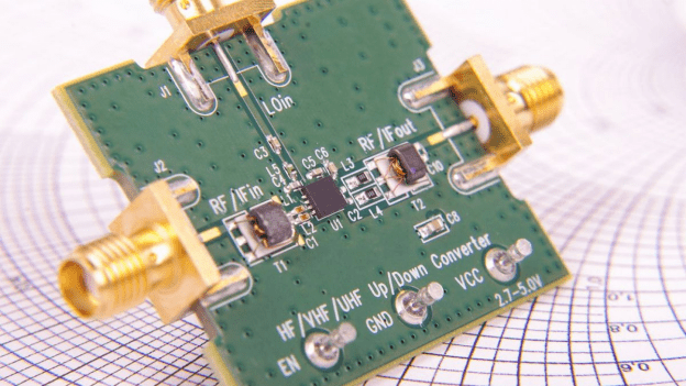
A Guide To The RF PCB Design
 hillmancurtis.com
A Guide to the RF PCB Design
PCB Layout Design - ESP32-C2 - — ESP Hardware Design Guidelines Latest
 docs.espressif.com
PCB Layout Design - ESP32-C2 - — ESP Hardware Design Guidelines latest ...
Guide To PCB Layout Design
 hillmancurtis.com
Guide to PCB Layout Design
How To Design A PCB Layout
 hilelectronic.com
How to Design a PCB Layout
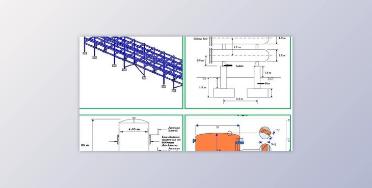
دانلود Onshore Structural Design–Step By Step Calculations
 gfxplugin.com
دانلود Onshore Structural Design–Step By Step Calculations
A Detailed Guide To PCB Layout Design |Qtech Technology Co. Ltd
 qtech-us.com
A detailed guide to PCB layout design |Qtech Technology Co. Ltd
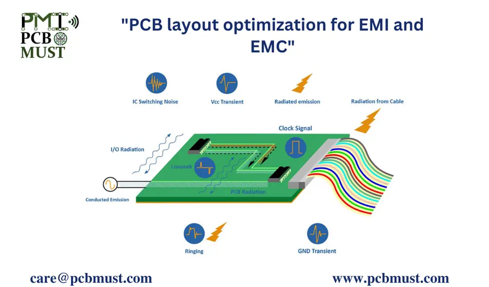
PCB Layout Optimization For EMI And EMC
 pcbmust.com
PCB Layout Optimization for EMI and EMC
Simple PCB Layout Design: Tips And Strategies
 resources.pcb.cadence.com
Simple PCB Layout Design: Tips and Strategies
Chassis Ground Pcb Layout At Theresa Troutman Blog
 storage.googleapis.com
Chassis Ground Pcb Layout at Theresa Troutman blog
[PDF] Intro To PCB Design: A Beginner’s Guide To Mastering PCB Layout
![[PDF] Intro to PCB Design: A Beginner’s Guide to Mastering PCB Layout](https://www.raypcb.com/wp-content/uploads/2023/02/PCB-Design-Guidelines-For-EMI-EMC.jpg) wiringtoolsreview.blogspot.com
wiringtoolsreview.blogspot.com
[PDF] Intro to PCB Design: A Beginner’s Guide to Mastering PCB Layout ...
25 Quick Mehndi Designs For Beginners - 2023 | Fabbon
 fabbon.com
25 Quick Mehndi Designs For Beginners - 2023 | Fabbon
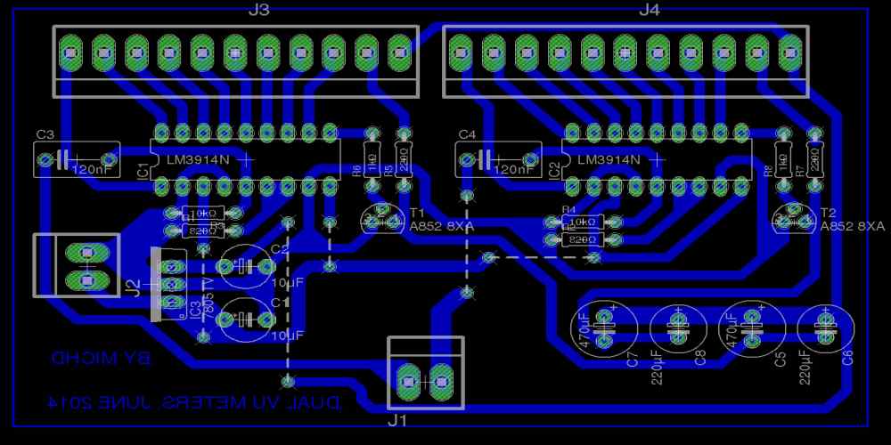
pcb layout design. Pcb layout design. Optimize your pcb trace using ipc-2152 standard